Table of Contents
ToggleWhat Is PCB?
A Printed Circuit Board (PCB) is a flat board made of non-conductive material, typically fiberglass, with conductive pathways etched or “printed” onto the surface. These pathways connect different points on the board, allowing electrical signals and power to be routed between various electronic components.
PCBs serve as the foundation for most electronic devices, providing a sturdy and organized platform for mounting and interconnecting electronic components. They are the backbone of modern electronics, enabling the miniaturization and integration of complex circuits.
Printed Circuit Board Applications
PCBs are used in virtually all electronic devices, including:
- Computers and laptops
- Smartphones and tablets
- Televisions and audio equipment
- Automotive electronics
- Industrial control systems
- Medical devices
- Aerospace and defense systems
- Renewable energy equipment
The versatility of PCBs allows them to be used in a wide range of applications, from consumer electronics to mission-critical industrial and military applications.
Types of PCBs
PCBs come in various types, each designed to meet specific requirements:
- Single-sided PCBs: Have conductive traces on one side of the board
- Double-sided PCBs: Have conductive traces on both sides of the board
- Multi-layer PCBs: Consist of multiple layers of conductive traces, separated by insulating layers
- Rigid PCBs: Made of rigid materials like FR-4 fiberglass
- Flexible PCBs: Made of flexible materials like polyimide, allowing them to bend and conform to various shapes
- Rigid-flex PCBs: Combine rigid and flexible PCB sections in a single board
The choice of PCB type depends on factors such as the complexity of the circuit, the required form factor, and the operating environment.
Materials Used
Common materials used in PCB manufacturing include:
- FR-4 (Flame Retardant 4): A composite material of woven fiberglass cloth with an epoxy resin binder, the most widely used PCB material
- Polyimide: Used for flexible PCBs due to its flexibility and high-temperature resistance
- Copper: The primary conductive material used for the traces on the PCB
- Solder mask: A protective coating that covers the copper traces, preventing short circuits
- Silkscreen: A printed layer that provides labels and markings for components and test points
The selection of materials is crucial for ensuring the PCB’s mechanical, electrical, and thermal performance.
Circuit Board Components
A bare PCB typically includes the following key components:
- Copper traces: The conductive pathways that interconnect the electronic components
- Pads and lands: Designated areas where components will be soldered or attached
- Vias: Plated-through holes that allow electrical connections between different layers of the PCB
- Solder mask: A protective coating that covers the copper traces
- Silkscreen: Printed labels and markings for component identification and test points
These basic components form the foundation of a PCB, enabling the integration and interconnection of electronic components.
What is a Printed Circuit Board Assembly?
Printed Circuit Board Assembly Definition
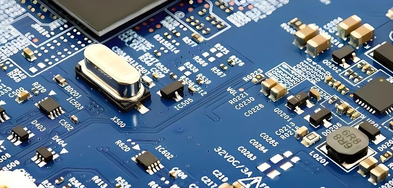
- A Printed Circuit Board Assembly (PCBA) is a PCB that has been populated with electronic components and soldered in place. It’s the final product that’s ready to be installed in an electronic device.
- The PCBA is the complete, functional circuit board that includes all the necessary components, such as resistors, capacitors, integrated circuits, and connectors, assembled and interconnected on the PCB.
Printed Circuit Board Assembly Benefits
- Increased reliability: The soldered connections provide a secure and durable attachment of components, improving the overall reliability of the electronic device.
- Compact design: The integration of components on a PCBA allows for a more compact and space-efficient design compared to individual components mounted on a breadboard or other prototyping platforms.
- Easier troubleshooting and repair: The organized layout and standardized connections of a PCBA make it easier to identify and replace faulty components.
- Consistent performance: The automated assembly process ensures consistent quality and performance across multiple units of the same PCBA design.
- Cost-effective for mass production: The automated assembly techniques used in PCBA manufacturing make it a cost-effective solution for high-volume production.
Printed Circuit Board Assembly Techniques
There are two primary techniques used in PCBA manufacturing:
What is Through-Hole Technology
Through-Hole Technology involves component leads being inserted through holes in the PCB and soldered on the opposite side. It provides stronger mechanical bonds for larger components and is often used for components that require higher power handling or thermal dissipation.
What is SMT (Surface Mount Technology)
SMT is a method for producing electronic circuits where components are mounted directly onto the surface of PCBs. It allows for smaller components and higher component density, enabling more compact and efficient designs.
Difference between PCBAs: THT Assembly, SMT Assembly and Mixed Technology
- THT Assembly: Uses through-hole components exclusively
- SMT Assembly: Uses surface-mount components exclusively
- Mixed Technology: Combines both THT and SMT components on the same board, taking advantage of the strengths of both techniques
The choice between these PCBA assembly methods depends on the specific design requirements, component types, and manufacturing capabilities.
Eight Key Steps in Printed Circuit Boards Assembly (PCBA) Process
Design for Manufacturability Check (DFM Check)
Ensures the PCB design can be manufactured efficiently and reliably, taking into account factors such as component placement, trace widths, and hole sizes.
Solder Paste Stenciling
Applies a precise amount of solder paste to the PCB, creating the attachment points for the components.
Pick and Place
Automated machines accurately place the electronic components onto the PCB, ensuring consistent and accurate positioning.
Reflow Soldering
The PCB is heated in a controlled environment, causing the solder paste to melt and form permanent connections between the components and the PCB.
Inspection and Quality Control
Automated optical inspection (AOI) and X-ray inspection are used to detect any defects or issues in the assembled PCBA.
Through-Hole Component Insertion
For boards with through-hole components, these are inserted manually or by specialized machines and then soldered in place.
Final Inspection and Functional Test
The assembled PCBA undergoes a final inspection and functional testing to ensure it meets the design specifications and operates as intended.
Washing and Drying
The PCBA is cleaned to remove any flux residues or other contaminants, ensuring the long-term reliability and performance of the assembly.
What is the Difference Between PCB and PCBA?
PCB: The bare board with conductive traces but no components
PCBA: The complete assembly with all components soldered in place
The key difference is that a PCB is the foundational substrate, while a PCBA is the fully assembled and functional circuit board ready for integration into an electronic device
How to Choose a High-Quality PCBA Supplier
Greenspcba Technology provides customers with leadership and experience in advanced PCB Assembly technology, with proven processes and a full range of services. From prototyping, low volume high mix to high volume global manufacturing, we provide Printed Circuit Board Assembly services for worldwide customers. Greenspcba is a recognized professional contract manufacturer, developing the latest PCBA and surface mount (SMT) capabilities

Recent Comments